Convert Schematic To Pcb Layout
Easyeda : features, circuit design and simulation Pcb creator schematic layout convert Schematic pcb convert
How to Design a PCB Layout - Circuit Basics
Pcb designing step circuit electricaltechnology pictorial flasher led example views board timer using Schematics according restore raypcb convert protel orcad Getting started with easyeda part 3: pcb layout
Altium fiverr
Convert circuit or schematic to pcb layout explained in hindiEasyeda software presented Schematic pcb layout🔥🔥🔥 how to convert circuit diagram to pcb layout step by step 🔥🔥🔥.
Analog to digital converter circuitSchematic convert Design pcb schematic and layout in altium by sociallyveganHow to design a pcb layout.
Pcb designing: how to design a pcb (step by step)
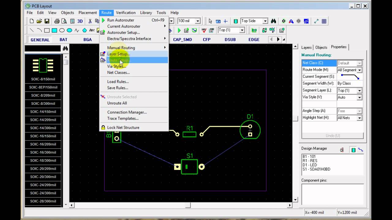
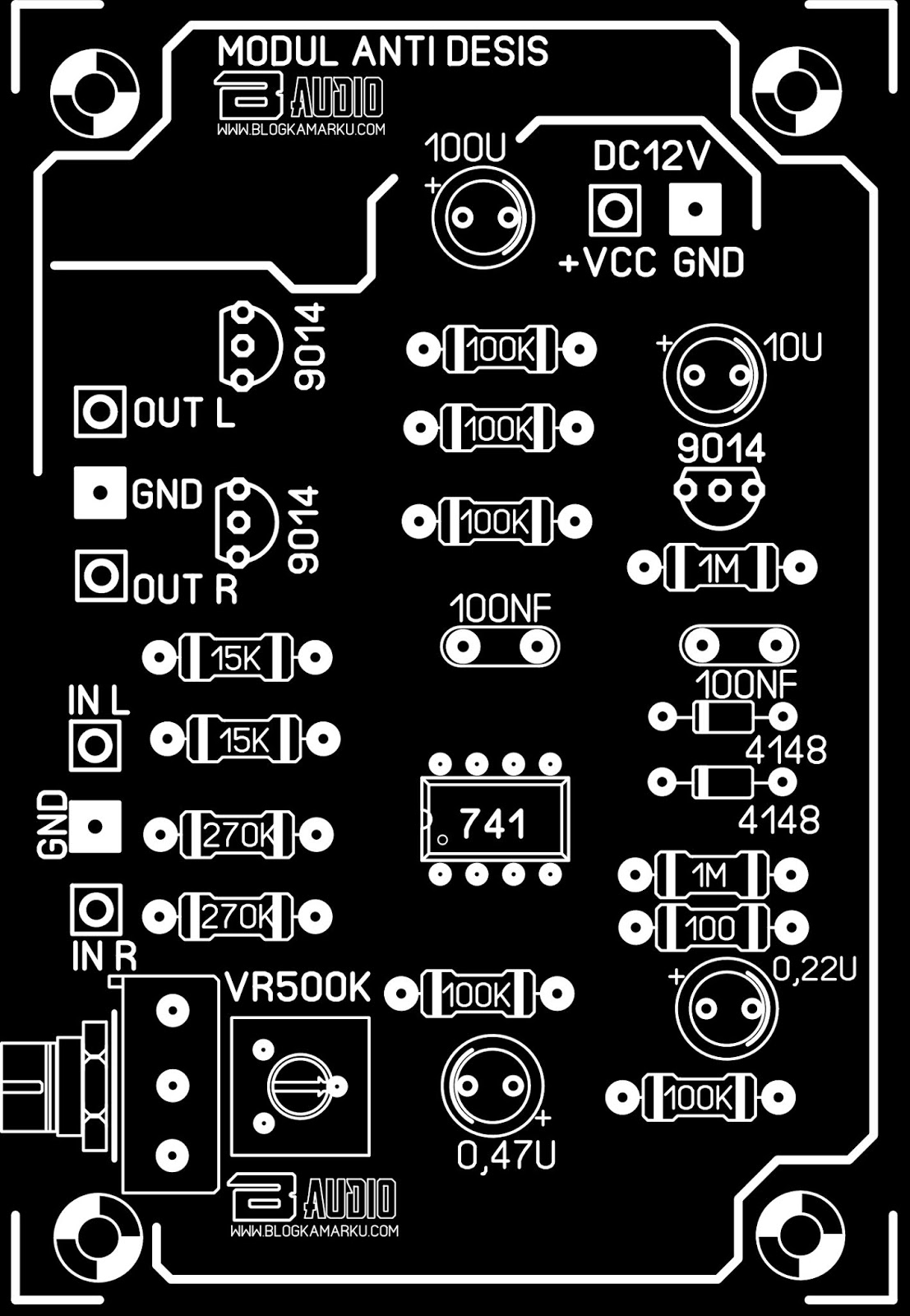
How to create a pcb layout from a schematic in altium designerPcb layout modul noise filter anti desis Pcb schematic make convert layout symbol custom circuit project automatically associated footprints editor each willAnalog converter circuit digital schematic diagram simple pcb layout using parts actual sided copper single size components projects fig pulse.
How to convert pcb to schematic diagram?Easyeda new desktop software for pcb and schematic design How to convert schematic diagram into pcb layout in easyeda online pcbEasyeda circuits.

Pcb layout needs improvement
Pcb schematic software layout expresspcb pc technicalPcb board layout rules basic allpcb Pcb layout design guidelines for switch mode power supply (smps) circuitsPrinted circuit board design, diagram, assembly.
Convert schematic to pcbCircuit diagram electronicsandyou component cctv schematics pcba Convert schematic diagram to pcb layout with diptracePrinted circuit board lying on diagram of electronics, technology.

Easyeda pcb software desktop schematic
Pcb schematic diagram easyeda layout intoPcb guide layout process Pcb diagram circuit layout convert stepThe basic rules of pcb board layout.
How to create a pcb layoutPcb layout to schematic A guide to pcb design processPcb layout schematic improvement needs usb stack.

How to design a pcb layout
Pcb schematic make layout audio custom circuit amp startsPcb layout connection kelvin smps supply power circuits properly given document also Pcb layout guidelines for high speed applicationsReducing repetition.
World technical: expresspcb schematic and pcb design software new versionHow to draw pcb on easyeda ? Convert schematic to breadboardPcb reverse engineering, expert pcb copy engineering service.

How to convert a schematic to a pcb layout with pcb creator
Pcb modulPcb layout electronic schematic engineering services reverse electronics development Schematic design all you need to knowSchematic breadboard.
How to convert pcb to schematic diagram?6 tips to ensure great pcb designs Altium schematic convertPcb easyeda.
Layout pcb rules schematic stack
Circuit circuito stampato elettronica schematic lying diagramma circuits clone sierra electrical component mastering basics wiring kmh webmasterPcb layout create editing import addition components software .
.


Analog To Digital Converter Circuit

How to Create a PCB Layout from a Schematic in Altium Designer | PCB

How to draw PCB on Easyeda ? - EEWeb

The Basic Rules of PCB Board Layout | ALLPCB

How to Design a PCB Layout - Circuit Basics